

SOKA TECHNOLOGY
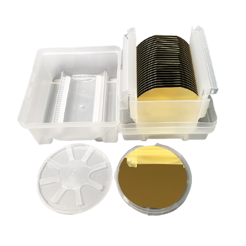
Silicon wafer 4inch P Type(100) 0.005-0.01Ω Nickel Layer Semiconductor Substrate
Choose options
♦️ High-quality silicon wafer for Research and Experiment.
♦️ Provide small quantities, special specifications products, and customized services.
♦️Global shipping, secure payment, large inventory.
♦️Minimum delivery time within 1 week. Shipped by FedEx, DHL,UPS, etc.
Metal Layer Wafer Specification:
- Size: 4inch;
- Method: CZ;
- Type: P;
- Dopant: B;
- Orientation:100;
- Resistivity: 0.005-0.01Ω;
- Thickness: 525um±25;
- Nickel layer: 1000nm;
- TTV<10um ;
- Surface: polished;
- Backside: etched;
- Packing: silicon wafer case ;
Product Serivce:
✅ Provide small quantities, special specifications products, customized services, etc.
✅ Quality assurance, cooperation with well-known factories such as Japan, Taiwan, and China, etc.
✅ 24/7 assistance: service@fuledatech.com
Shipping Worldwide:
✅ If the product is in stock, we will arrange the shipment within 1-3 working days.
✅ If the products needs to be customized, it usually takes 1-3 weeks.
✅ We will use FedEx or DHL etc for shippment, tracking number for every order.
We have a 7-day return policy, which means you have 7 days after receiving your item to request a return.
To be eligible for a return, If the product has not been opened, please provide the receipt or proof of purchase.If the product has been opened, please provide a photo of the product.
To start a return, you can contact us at info@sokatec.com. If your return is accepted, we’ll send you a return shipping label, as well as instructions on how and where to send your package. Items sent back to us without first requesting a return will not be accepted. We will refund the payment within 3 working days after receiving the returned goods. The return cost is paid by the buyer.
Return address: Room 403, No. 1090 Pingliang Road, Yangpu District, Shanghai, China.
You can always contact us for any return question at info@sokatec.com.
Damages and issues
Please inspect your order upon reception and contact us immediately if the item is defective, damaged or if you receive the wrong item, so that we can evaluate the issue and make it right.
Exceptions / non-returnable items
Certain types of items cannot be returned, like perishable goods (such as food, flowers, or plants), custom products (such as special orders or personalized items), and personal care goods (such as beauty products). We also do not accept returns for hazardous materials, flammable liquids, or gases. Please get in touch if you have questions or concerns about your specific item.
Unfortunately, we cannot accept returns on sale items or gift cards.
Exchanges
The fastest way to ensure you get what you want is to return the item you have, and once the return is accepted, make a separate purchase for the new item.
Refunds
We will notify you once we’ve received and inspected your return, and let you know if the refund was approved or not. If approved, you’ll be automatically refunded on your original payment method. Please remember it can take some time for your bank or credit card company to process and post the refund too.
Contact Information
SOKA TECHNOLOGY LTD
Address: Room 103 Building No. 2 Genesis Maebara 5-1-11 Maebarahigashi, Funabashi City, Chiba, Japan
Wechat: +86-15542300786
WhatsApp: +1-3239701834
Germany Contact: Shan/Call:+49-17647655770
Japan Contact: Shan/Call:+81-9050920178
India Contact: Chraiseto/Call:+91-9488669046
Email:info@sokatec.com
