

SOKA TECHNOLOGY
Silicon wafer 4inch P Type(100) 0.005-0.01Ω Nickel Layer Semiconductor Substrate
オプションを選択
♦️ High-quality silicon wafer for Research and Experiment.
♦️ Provide small quantities, special specifications products, and customized services.
♦️Global shipping, secure payment, large inventory.
♦️Minimum delivery time within 1 week. Shipped by FedEx, DHL,UPS, etc.
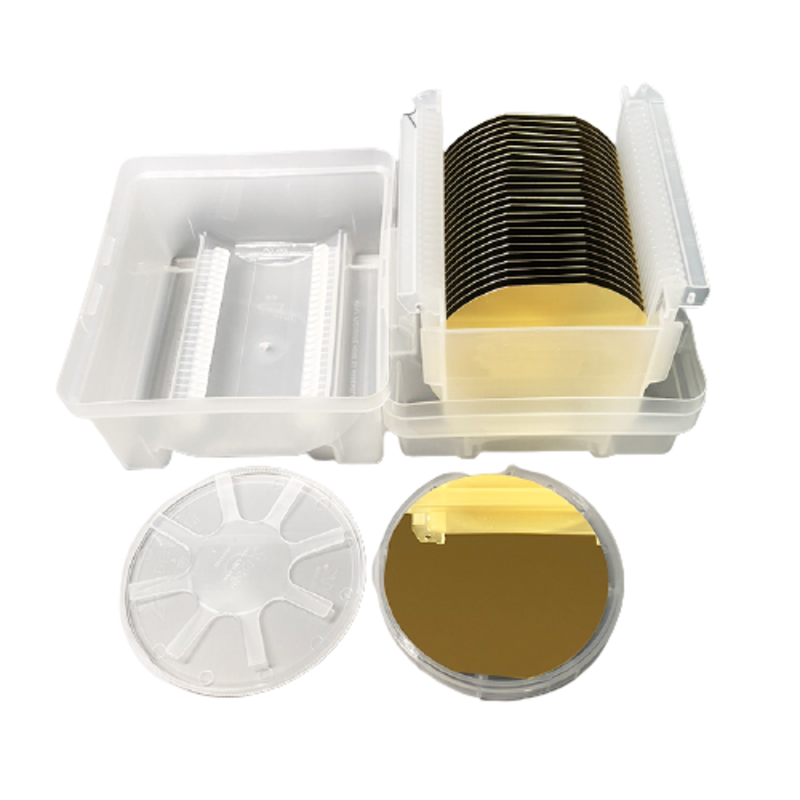
Metal Layer Wafer Specification:
- Size: 4inch;
- Method: CZ;
- Type: P;
- Dopant: B;
- Orientation:100;
- Resistivity: 0.005-0.01Ω;
- Thickness: 525um±25;
- Nickel layer: 1000nm;
- TTV<10um ;
- Surface: polished;
- Backside: etched;
- Packing: silicon wafer case ;
製品サービス:
✅少量、特殊仕様品、カスタマイズサービス等を提供します。
✅品質保証、日本、台湾、中国などの有名工場との提携など。
✅年中無休のサポート:service@fuledatetech.com
世界中への配送:
✅在庫がある場合は、1~3営業日以内に発送手配させていただきます。
✅製品をカスタマイズする必要がある場合、通常は 1 ~ 3 週間かかります。
✅ 発送にはFedExまたはDHLなどを使用し、すべての注文の追跡番号を使用します。
当社では 7 日間の返品ポリシーを設けており、商品を受け取ってから 7 日以内に返品をリクエストすることができます。
返品をお受けするには、商品が未開封の場合は領収書または購入証明書をご提示ください。商品が開封されている場合は、商品の写真をご提供ください。
返品手続きを開始するには、 info@sokatec.comまでご連絡ください。返品が承認された場合、返品用送り状と、荷物の送付方法および送付先に関するご案内をお送りします。返品のお申し出なくご返送いただいた商品は、お受けできません。返品商品到着後3営業日以内に返金いたします。返送費用はお客様のご負担となります。
返送先住所:中国上海市楊浦区平涼路1090号403号室。
返品に関するご質問は、いつでもinfo@sokatec.comまでお問い合わせください。
損害と問題
商品を受け取ったらすぐに注文内容を点検し、商品に欠陥や破損がある場合、または間違った商品を受け取った場合は、すぐに当社にご連絡ください。当社が問題を評価し、対応いたします。
例外 / 返品不可商品
生鮮食品(食品、花、観葉植物など)、カスタム商品(特注品やパーソナライズ商品など)、パーソナルケア商品(化粧品など)など、一部の商品は返品できません。また、危険物、可燃性液体、ガスの返品もお受けできません。特定の商品についてご質問やご不明な点がございましたら、お気軽にお問い合わせください。
申し訳ございませんが、セール品やギフトカードの返品はお受けできません。
取引所
ご希望の商品を確実に手に入れる最も早い方法は、お持ちの商品を返品し、返品が承認されたら新しい商品を別途購入することです。
払い戻し
返品を受け取り、検査が完了したら、返金の可否をご連絡いたします。返金が承認された場合は、元のお支払い方法で自動的に返金されます。銀行またはクレジットカード会社による返金処理と反映には、多少お時間がかかる場合がございますのでご了承ください。
連絡先
創価学会 テクノロジー株式会社
住所:千葉県船橋市前原東5-1-11 ジェネシス前原2号館 103号室
微信: +86-15542300786
WhatsApp: +1-3239701834
ドイツ連絡先:Shan/電話: +49-17647655770
日本連絡先:Shan/電話: +81-9050920178
インド 連絡先: Chraiseto/電話: +91-9488669046
メールアドレス:info@sokatec.com
